큰 구리 영역은 반대쪽 레이어의 "copper filling"으로 균형을 맞춰야 합니다. 또한 가능한 Copper Trace를 보드 전체에 최대한 균일하게 분포시키십시오. (고주파 설계와 관계 없다면) 다층 회로 기판(Multi layer board)의 경우 반대쪽 레이어와 Copper가 대칭하도록 "Copper Filling (구리 채우기)"을 합니다.
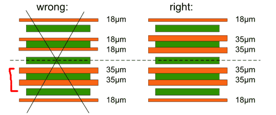
3. Copper foil(동박)의 두께는 상하 Layer에 대해 항상 대칭적으로 분포
회로 기판의 레이어 빌드업에서 Copper foil(동박)의 두께는 항상 대칭적으로 분포되어야 합니다. 물론 비대칭 레이어 빌드업을 제작할 수 있지만, 변형 가능성 때문에 이러한 설계는 지양하는 것이 좋습니다.
I am often reminded of their tunneling when I am routing a printed circuit board with high density ball grid array (BGA) parts on it. Routing the signal traces out of the BGAs is a process that is generally referred to as “escape routing.” With the more dense parts however, this can be a real challenge. You typically have to plan out ahead of time where the routes must go, change the trace widths to a smaller size in order to fit, and tunnel through the board using a variety of vias. To get all the nets successfully routed out of a BGA can end up being “a great escape” in its own rights. Here are some techniques that can help you with your BGA escape routing.
* 터널링 : 구멍 뚫는 것
고밀도 볼 그리드 배열(BGA) 부품이 있는 인쇄 회로 기판(PCB)을 배선할 때 종종 터널링이 생각납니다.
신호 트레이스를 BGA 밖으로 라우팅하는 것은 일반적으로 "Escape Routing"이라고 불리는 프로세스입니다.
그러나 부품이 더 조밀해지면, 이것은 진짜 어려운 과제가 될 수 있다.
일반적으로 배선이 어디로 가야 하는지 미리 계획해야 하고, 배선의 너비를 적합하도록 더 작은 크기로 변경하고, 다양한 비아를 사용하여 보드를 통과해야 합니다.
BGA에서 모든 네트를 성공적으로 라우팅하는 것은 결국 그 자체로 "성공적인 탈출"이 될 수 있다.
다음은 BGA 이스케이프 라우팅에 도움이 될 수 있는 몇 가지 기술입니다.
Component Placement: The Essential First Step to Successful BGA Escape Routing
To successfully route out of large scale fine pitch parts requires a good component placement to begin with. As with any board, start with the fixed components like connectors first. Next, locate the major components such asyour BGAsaccording to their connectivity. You certainly need to be aware of any thermal issues with the board as well as high speed needs so that you don’t place sensitive components in too hot or noisy areas of the board. Once those parts are placed, then you can focus on how best to place the rest of the board to help with your escape routing:
Keep the decoupling capacitors as close as possible to the pins on the BGA that they will connect to. This will help to keeptheir inductancelow, and allow you to place them so that they won’t get in the way of your routing.
Place components according to their signal paths. Not only is this important forhigh speed signal performance, but again by placing those first you will give yourself more room for routing later.
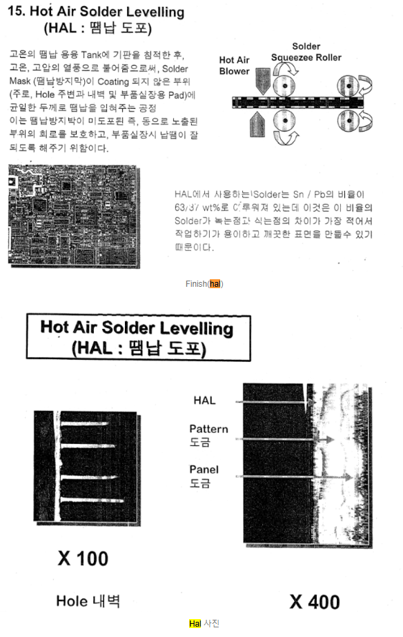
Spread out your placementenough to fit in the escape routing that you are going to be doing. Here is where you will have to find a good compromise in your placement. You need to place your parts so that they are positioned optimally for their performance, while at the same time leaving yourself room for all of the routing that you will be doing.
Once you are placed, it’s time to work on the escape routing.
부품 배치: 성공적인 BGA 탈출 라우팅을 위한 필수 첫 단계
어딘가에 터널을 뚫는다는 것은 그곳에 터널을 만드는 것을 의미합니다.
구성 요소 배치: 성공적인 BGA 탈출 라우팅을 위한 필수 첫 단계 대규모 미세 pitch(pin사이 간격이 좁음) 부품에서 성공적으로 라우팅하려면 먼저 좋은 구성 요소 배치가 필요합니다.
다른 보드와 마찬가지로 먼저 커넥터와 같은 고정 구성 요소부터 시작합니다. 그런 다음 연결에 따라 BGA와 같은 주요 구성 요소를 찾습니다. 보드의 너무 뜨겁거나 시끄러운 영역에 민감한 구성 요소를 배치하지 않도록 보드의 열 문제와 고속 요구 사항을 확실히 알고 있어야 합니다. (보통 시뮬레이션을 통해 배치위치를 찾아냄)
이러한 부품(민감한 부품들 먼저)이 배치되면, Escape Routing을 위해 나머지를 배치하는 가장 좋은 방법에 집중할 수 있습니다.
디커플링 커패시터를 연결할 BGA의 핀에 가능한 한 가깝게 유지하십시오. 이렇게 하면 인덕턴스를 낮게 유지하고 라우팅을 방해하지 않도록 배치할 수 있습니다.
신호 경로(신호가 흐르는 방향)에 따라 부품 배치합니다. 이것은 고속 신호 성능에 중요할 뿐만 아니라, 이를 먼저 배치함으로써 나중에 라우팅을 위한 더 많은 공간을 확보할 수 있습니다.
수행하려는 Escape Routing에 맞게 배치를 분산하십시오. 여기에서 배치에서 적절한 절충안을 찾아야 합니다. 성능에 가장 적합한 위치에 부품을 배치하는 동시에 수행할 모든 라우팅을 위한 공간을 확보해야 합니다.
배치가 되면 Escape Routing를 작업할 시간입니다.
부품을 배치한 상태에서 BGA에 대한 이스케이프 라우팅을 시작할 수 있습니다.
반응형
Tunneling to Freedom: How Best to Work with Traces and Vias for BGA Escape Patterns
Let’s start with the trace routing of a BGA escape pattern first:
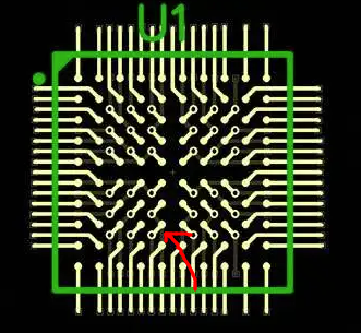
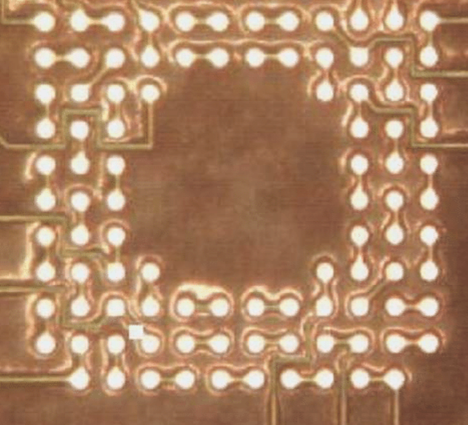
The first thing that you can do, which is the simplest, is to route your escapes out from the outer rows of the BGA. This is usually done diagonally to give yourself more routing channels.
For larger parts with enough space between the pins, escape routing is usually done in a dog bone pattern. This is a short trace that directly connects the BGA pad to the via immediately next to it. You may also route inward on a BGA package to vias in the center.
Once the pin pitch begins to shrink on the larger BGAs, the escape routing becomes more difficult. One tactic is to shrink the trace widths down, although you don’t want to get any smaller than 0.003 inches. Depending on the pitch of the part, this should allow for more routing between the BGA pads.
자유로의 터널링: BGA 이스케이프 패턴을 위한 트레이스와 비아로 작업하는 가장 좋은 방법
먼저 BGA Escape 패턴 라우팅부터 시작하겠습니다:
가장 간단한 방법으로 할 수 있는 첫 번째 일은 BGA의 바깥쪽 행에서 Escape Routing 경로를 지정하는 것입니다. 이것은 일반적으로 더 많은 라우팅 채널(channel : pin 사이 공간)을 제공하기 위해 대각선으로 수행됩니다..
또는 핀 사이에 충분한 공간이 있는 더 큰 부품, Escape Routing는 일반적으로 개 뼈 패턴(Dog bone pattern)으로 수행된다. 이것은 BGA 패드를 바로 옆에 있는 비아에 직접 연결하는 짧은 배선입니다. 또한 BGA 패키지에서 중앙의 비아로 안쪽으로 라우팅할 수 있습니다.
더 큰 BGA에서 핀 pitch(=핀 사이 간격)가 줄어들기 시작하면 Escape Routing이 더 어려워집니다. 0.003인치보다 더 작아지고 싶지는 않겠지만, 한 가지 방법은 폭을 더 줄이는 것이다. 부품의 피치에 따라 BGA 패드간에 더 많은 라우팅이 가능해야 합니다.
dog bone pattern (pan out) 개뼈처럼 생겼다고 해서
Along with your trace routing, you will also be placing the vias. Here are some via considerations to keep in mind:
On small BGAs with only a few rows, your regular routing vias will probably work fine. On larger BGAs though, you may need to shrink the vias in order to fit them within the BGA pattern.
In dense BGAs a very helpful option is to place your vias in the component pads. This will free up a lot of space on the board but may cause manufacturing difficulties. Make sure that your manufacturer is on-board with this plan first.
Another option is touse micro-vias. These are often used when the BGA pad pitches decrease to 0.5 millimeters. Micro-vias can be as small as .004 inch holes with a pad size of .008. Be warned though, using micro-vias will raise the cost of manufacturing your board.
배선과 함께 비아도 배치합니다. 아래는 비아(via) 배치시 염두에 두어야 할 몇 가지 고려 사항입니다:
행(row) 수가 적은 작은 BGA에서는 일반 라우팅 비아가 잘 작동할 것입니다. 그러나 더 큰 BGA에서는, BGA 패턴 내에 비아(via)를 맞추기 위해 비아를 축소(크기나 갯수 등)해야 할 수도 있습니다.
고밀도 BGA에서 매우 유용한 옵션은 구성 요소 패드(pad)에 비아(via)를 배치하는 것입니다. 이렇게 하면 보드에서 많은 공간이 확보되지만 제조상의 어려움이 발생할 수 있습니다. 먼저 제조업체가 이 계획에 참여하고 있는지 확인하십시오.
또 다른 옵션은 마이크로비아(microvia : 레이저를 사용한 매우작은 via)를 사용하는 것입니다. 이들은 BGA 패드 피치(pad pitch = pad간 사이간격)가 0.5mm로 아래로 감소할 때 자주 사용됩니다. 마이크로비아는 패드 사이즈(pad size)가 .008inch(=0.2032mm)인 0.004inch(=0.1016mm) 구멍만큼 작을 수 있습니다. 그러나 마이크로비아를 사용하면 보드 제조 비용이 증가할 수 있습니다.
Ultimately the escape routing strategy that you choose will depend on the BGA pad pitch, the size of the BGA part, the overall routing density of the board, and the size of traces and vias that you use.
Large fine-pitch BGAs will typically require more board layers as you will usually have room to only escape route a couple of rows of pads to a single board layer.
Additional board layers will mean additional cost however, and may impact the signal integrity of your design. Once again, make sure that you check into all of these factors before you commit.
궁극적으로 선택하는 Escape Routing 전략은 BGA Pad Pitch (pad간 간격), BGA Part의 크기, 보드의 전체 라우팅(배선) 밀도, 사용하는 배선두께(trace width)와 비아(via)의 크기에 따라 달라집니다.
큰 미세 피치 BGA(large fine-pitch BGA)는 일반적으로 몇 줄의 패드를 단일 보드 레이어로 탈출할 수 있는 공간이 있기 때문에 일반적으로 더 많은 보드 레이어가 필요합니다.
그러나 추가 보드 레이어(layer를 늘리기)는 추가 비용을 의미하며, 설계의 신호 무결성에 영향을 미칠 수 있습니다. 다시 한 번, 커밋하기 전에 이러한 모든 요소를 확인하십시오.
Tips For a Great Escape
One of the best resources that you can turn to is the component vendor’s data sheets for the BGA parts that you are working with. Often you will find recommended escape routing patterns that can save you a lot of time. Another good resource is to work ahead with your PCB manufacturer. They can advise you on the best board layer configuration for your high speed design needs, as well as thesize and type of tracesand vias that you can safely use for routing your BGAs.
Another helpful tip is to maximize the use of your PCB design tools. Your design tools will have the capabilities to shrink traces and automatically change via sizes within a specified area that you can set up around your BGAs. They also will have features allowing you to set up the high-speed design rules and other requirements of your board.
Great Escape(멋진 BGA배선으로 부터 탈출) 하기 위한 팁!
참고할 수 있는 최고의 리소스 중 하나는 작업 중인 BGA 부품에 대한 부품 공급업체의 데이터 시트입니다.
종종 많은 시간을 절약할 수 있는 권장 탈출 경로 패턴(escape routing patterns)을 찾을 수 있습니다. 또 다른 좋은 리소스는 PCB 제조업체와 협력하는 것입니다.
-> 제조사의 Datasheet에 권장하는 Escape Routing Pattern을 안내
BGA 라우팅에 안전하게 사용할 수 있는 트레이스(trace = 배선) 및 비아(via)의 크기와 유형(type)뿐만 아니라 고속 설계 요구에 가장 적합한 보드 레이어(board layer) 구성에 대해 조언할 수 있습니다.
Another helpful tip is to maximize the use of your PCB design tools.
Your design tools will have the capabilities to shrink traces and automatically change via sizes within a specified area that you can set up around your BGAs. They also will have features allowing you to set up the high-speed design rules and other requirements of your board.
또 다른 유용한 팁은 PCB 설계 도구(EDA 소프트웨어)의 사용을 극대화하는 것입니다.
디자인 도구(EDA PCB 설계 툴)에는 트레이스(trace)를 축소하고 BGA 주변에 설정할 수 있는 지정된 영역 내에서 크기를 통해 자동으로 변경하는 기능이 있습니다. (Constraint Region Rule 같은...)
또한 보드의 고속 설계 규칙(Contraint Electrical Rule 같은...) 및 기타 요구 사항을 설정할 수 있는 기능도 있습니다.