도로체증이 심한곳에는 소통을 원활하게 하기 위해 우회도로같은 것이 있듯이, 회로나 시스템에서도 신호를 우회시켜야 할 경우가 있는데 이런 경우 전반적으로 사용되는 용어이다. (굉장히 다양하게 사용됨)
통신시스템의 경우 본회로가 고장났을때 즉시 스위치에 의해 연결되는 대체회로를 bypass circuit이라고 부르기도 한다.
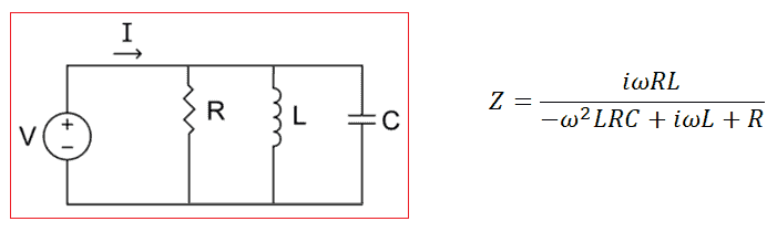
아마 bypass는 회로내의 전원단에서 많이 보게 될텐데, 주로 AC전원이 DC로 타고드는 것을 방지하기 위해 사용된다.
Tr등에 DC전원을 입력할때, RF신호가 DC입력단으로 새지 않도록 inductor나 1/4파장 선로등을 써서 RF choke 역할을 하게 하지만, 100% 완벽하게 막아내지는 못한다. 그렇게 해서 조금씩 새어나온 RF신호는 DC입력전원으로 타고들어 공통 ground를 타고 loop를 만들면서 발진을 발생시킨다. 초크 특성상 원래 주파수보다 저주파의 신호가 주로 이렇게 새서 발진하게 되며, 이것을 막기위해 DC전원 입력옆에 병렬로 capacitor를 달아서 RF신호를 접지시켜버리는데, 이것을 소위 bypass시킨다고 한다.
capacitor는 DC는 통과하지 못하고 RF AC신호는 통과되며, capacitor의 값에 따라 얼마나 잘 통과되느냐가 결정된다. 이것은 Z = 1/jwC 의 임피던스 수식에 의해 해당주파수에서 낮은 임피던스를 가지도록 값을 정하지만, 실제로는 회로와 함께 복합적으로 어느 주파수의 발진이 심한지를 찾아내서 실험적인 값을 쓰는 경우가 많다.
즉 DC전원단으로 흘러들어갈 뻔한 RF신호를 옆의 capacitor로 흘러가게 하여 접지시켜 죽인다는 의미에서 bypass capacitor라는 식으로 bypass란 단어가 사용되는 것이다.
RF에서 bypass는 이러한 DC단의 RF신호 제거용 및 대체회로, 대체경로를 의미하는 용어로 많이 사용된다.
흔히 회로도에 전원단이나 Digital Logic 단에 bypass C를 다는 경우가 있다. 이는 RF 신호를 bypass 시키는 역활을 하고 , 또한
디지털 회로의 고유 특성때문에 턴온(L->H) 시간보다 턴오프(H->L) 시간이 더 길고 또한 TR에 기생되는 C 에 전압이 충전되 급변하지 않으므로 아주 짧은 시간동안 디지털 IC 내부에 TR 2개가 동시에 On 되는 경우가 있다. 이 현상은 전원에 순간적인 전류 스파이크를 일으키는데 이를 방지 하기 위해 TTL 소자의 주변에 bypass Cap 를 달아준다
반응형
=================================================
또한 아래 영문 자료에서도 유용한 부분이 있어 가져왔다.
Bypass capacitor는 가끔 Decouple Capacitor (Decap)과 혼용해서 사용하기도 한다.
A bypass capacitor is a capacitor that shorts AC signals to ground, so that any AC noise that may be present on a DC signal is removed, producing a much cleaner and pure DC signal.
A bypass capacitor essentially bypasses AC noise that may be on a DC signal, filtering out the AC, so that a clean, pure DC signal goes through without any AC ripple.
Bypass capacitor는 AC신호를 Gound로 단락(short)시켜 DC신호에 존재 할 만한 모든 AC노이즈를 제거하여 깨끗하고 순수한 DC 신호를 만들기 위한 capacitor입니다.
Bypass capacitor는 기본적으로 DC신호에 있을 수있는 AC노이즈를 우회시켜 AC를 필터링하여 깨끗하고 순수한 DC 신호가 AC ripple(DC신호에 남아있는 찌꺼지 노이즈) 없이 통과합니다.
실제 노이즈 있는 DC를 최대한 노이즈를 제거함
AC 노이즈(ripple)을 우회시킴 RE는 pure DC만 공급
So a bypass capacitor blocks the DC from entering it by the great resistance it offers to the signal but accepts the AC noise that may be on the DC line and shunts or bypasses it to ground. This is how bypass capacitors work.
그래서 bypass capacitor는 DC에 대해서는 크게 저항하고, 오직 AC노이즈만 받아들여 Gound로 우회시켜 보냄으로써 이러한 원리로 동작한다.
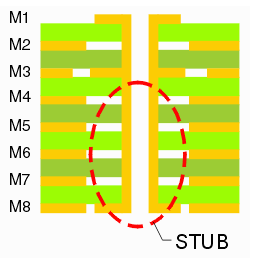
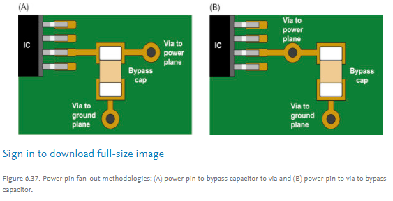
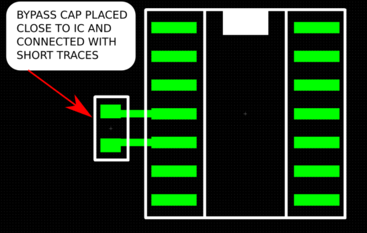
Bypass Cap는 IC와 최대한 가까이 배치, VCC와 GND핀의 의 Trace는최대한 짧게
BYPASS CAP VALUE AND SIZE:
Considering the impedance of the traces on the PCB, the input impedance of the IC, and the operating frequency of the IC, an optimal value of bypass capacitor does exist but going through the rigors of calculating the value is rarely useful or necessary. In many cases the datasheet for an IC will give a recommended value for the capacitor. If no value is suggested,0.1uF (100nF)is widely accepted as a standard go-to value. For most designs, a standard ceramic 0402, 0603, or 0805 package size will typically work well as a bypass cap.
BYPASS CAP 값 및 사이즈:
PCB Trace 임피던스, IC의 input 임피던스와 IC의 동작주파수를 고려하여 Bypass Cap의 최적의 값은 존재하긴 하나, 대부분 권장사항 값으로 0.1uF (100nF)가 표준값으로 사용됨. 대부분 설계 표준사이즈로는 0402, 0603, 0805 패키지(Footprint)를 사용하고, Bypass Cap으로 역할을 잘 수행함.
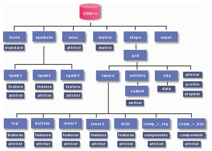
ODB++ is a printed circuit board manufacturing database originally developed by Valor. It was created to try to bring some order to the transfer of board data from the designers to the manufacturer. Because Valor also provides the dominant CAM tool to manfacturers the company was able to get the major industry players to adopt their proprietary standard. In recent years ODB++ has become more open after attempts by the IPC were made to replace it.
The great majority of PCB design software (layout) can output a valid and correct ODB++ file. A free ODB++ viewer can be obtained from Valor (Mentor) that allows one to visualize the data.
ODB++란?
ODB++는 원래 Valor(지금의 Mentor / Simense EDA)에서 개발한 PCB 데이터베이스 이다.
설계자로부터 PCB 제조를 위한 데이터 전송 순서를 정하기 위해 만들어짐.
당시 Valor는 CAM 툴의 독점적으로 점유하고 있기에 대부분의 산업군들이 ODB++ 방식을 채택함.
대부분 PCB설계 툴에서는 ODB++ 데이터를 출력할 수 있음. 이를통해 Valor(Mentor) 에서는 이 데이터를 시각화할 수 있으며, 무료 ODB++ 뷰어도 볼 수 있음
What Design Data is Needed to Make a PCB?
To actually build a PCB board the manufacturer needs quite a few pieces of data from the designer. I've summarized the data and its function below:
PCB제작을 위해 필요한 데이터는 무엇일까?
실제 PCB 보드제작을 위해서는 아래와 같은 사항의 데이터들이 필요함.
Gerber Files - these are actually "CNC" files which drive a photoplotter which creates the film used to expose each conductor layer in the board. There is also a Gerber file needed for other processes such as solder masks on top and bottom, paste masks and silk screens. So a four layer board could have 8-10 gerber files associated with it.
거버파일
실제 보드의 도체부분의 필름을 생성시키기 위한 포토플로터의 파일은 "CNC"파일이다.
또한 거버파일은 솔더마스크, 페이스트마스크, 실크스크린 등의 가공을 위한 파일이기도 하다.
그래서 만약 4개 layer라고 하더라고 실제는 8~10개 정도의 필름 레이어가 더 필요하다.
Drill Files - these are CNC files very similar to Gerber (but different) that are used to control a drilling machine. Plated through holes have to be drilled. On multi-layer boards you can have some holes that go all the way through, some that only go through a few layers and such. These each require a different drill file. There are lots of aggravations with drill data - first, there is no consistent standard as to how the drill tools should be defined in the header; second the coordinate system of the drill data can sometimes be offset from the Gerber files. Finally, one needs a separate document that describes which file passes through which conductor layers.
드릴 파일
거버파일과 매우 유사한 형태로 드릴가공을 위한 CNC파일이다. (그렇다고 동일하진 않음)
완전히 관통하는 through-hole 또는 일부 layer만 가공되는 Blind/Buried 일 수 있다. 이때는 각각 서로 다른 드릴정보가 필요하다.
둘째, 드릴 데이터 좌표가 거버파일로부터 약간 Offset 될 수 있음 (좌표가 살짝 벗어나는 것)
샛째, 어떤 파일이 어떤 conductor layer를 지나는지 설명하는 데이터가 필요한데 부족하다.
Routing Files - similar to drill files but defines a path for routing out the board.
라우팅 파일 (배선 파일)
드릴파일과 유사하지만, 이는 배선을 위한 경로를 정의
stackup - the stackup is generally a print or written description of the board material, thickness, interposer and order. It is essential for multi-layer boards.
Stackup (스택업)
다층기판에 필요한 보드의 재료, 두께, layer사이에 끼어있는 것들(Interposer), 쌓는 순서에 대한 정보
IPC-D-356 - esentially an electrical database of connections needed for testing the completed board. It is a very old format with a couple of variations and contains net names, test points and pins. Again, sometimes the data on this file is offset from the Gerbers which require manual intervention when trying to use this data.
IPC-D-356
완성된 PCB를 전기적 연결성을 테스트하기 위한 데이터베이스.
Net이름, TP(테스트포인트), 핀, Via 등에 대한 포맷
몇몇 데이터는 Gerber파일에서 offset이 되어 좌표를 벗어날 수 있으므로, 수동으로 조정이 필요
Documentation - describes key elements of the board (i.e. locations), dimensions, materials and such. It can take the form of a PDF file, an HPGL file, Gerber file or AutoCAD file.
문서화
좌표, 치수, 재료 같은 PCB의 핵심적인 요소 설명.
PDF나 HPGL파일, 거버파일, 오토캐드 파일 등으로 출력할 수 있음
Component Placements - this is not used by the bare board manufacturer but is used for DRC checking and for generating pick and place files. The component "library" is located in the EDA directory (as data) and the component placements are in the layer section: comp_ _top for the components on the top side and comp_ _bot for the componens on the bottom side.
부품파트 배치
보드만을 제작하는 업체는 사용하지 않지만, DRC검사 및 Pick & Placement 파일 생성에 필요
부품파트의 라이브러리는 각 EDA 디렉터리에 저장되어 있음.
Layer의 위치에 따라 comp_ _top 또는 comp_ _bttom 등과 같이 구성되어 있음
Importing and Checking
You can see that there is a lot of data to send from design to manufacturing and often the data that is transmitted is incomplete, inconsistent or just plain incorrect. So the first thing the board manufacturer does is to import all the different data formats and bring the data up in his CAM software. He then checks the data and runs a series of tests to insure that the board can be manufactured. If he finds violations such as traces too close, pads to small for the drill hole or other related problems he can either fix them or report them back to the designer.
Import(가져오기) 및 Checking(검사하기)
설계부터 제조까지 보낼 데이터는 많고 데이터가 부정확한 경우가 많음.
따라서 설계업체가 다양한 형식을 가공에 용이하게 CAM에 맞게 데이터를 출력할 필요가 있음
그 데이터들이 각 테스트를 통해 보드제조가 가능한지 확인해야 함.
검토과정에 제조할 수 없는 "너무 가까운 배선", "드릴 뚫기엔 너무 작은 구멍"와 같은 위반사항을 발견 시 수정할 필요가 있음.
이때 설계자는 해당 데이터를 수정할 필요가 있음
ODB++ provides a stable framework for the required data. It does not insure, of itself, that the data is correct or manufacturable but it does allow the board manufacturer to load all the data at once and immediately run the tests necessary to determine that it is consistent and buildable.
ODB++는 요구하는 데이터에 대해 안정적인 프레임워크(기준점?)를 제공함.
데이터 자체가 정확한 제조 가능성을 보장하지 않지만, 모든 제조업체가 한번에 데이터를 로드하여 제조 가능성을 평가할 수 있는 일관성을 제공.
What goes into the ODB++ is generally controlled by the PCB design tool and to a lesser extent by the designer. ODB++ has a lot of data "containers" that are optional and which may or may not be used by the exporting design tool.
ODB++는 설계자의 영향은 최소화 되며, PCB설계 툴에 의해 컨트롤 됩니다. (인간의 영향 최소화)
ODB++는 선택적으로 여러 데이터를 넣을 수 있고, 뺄 수도 있습니다.
The ODB++ File Structure
ODB++ is not a single "file" except when transmitting it from one place to another. To send an ODB++ file one first combines the files/directories into a tarball (this is an old Unix construct) and then zips it using gzip. However it is also possible to use other zip formats as long as the hierarchy (folder) structure is preserved.
ODB++ 파일 구조
ODB++는 통체로 보내는 것을 제외하고, 하나의 파일 (single file)이 아니다.
ODB++를 전송하기 위해서는 Tarball로 묶고 (유닉스/리눅스 기준), gzip을 통해 압축한다.
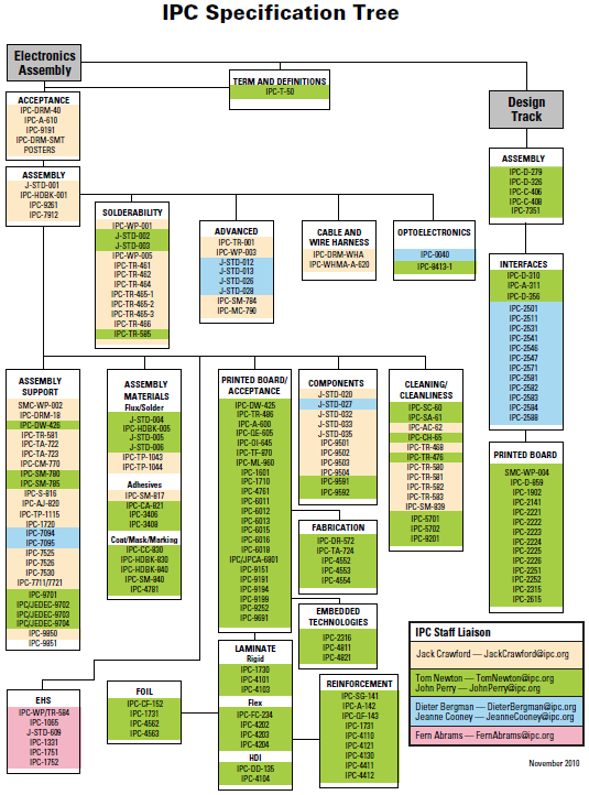
IPC또는국제전자산업표준협회(영어:Association Connecting Electronics Industries)는 전자장비 및 소자부품의 조립 및 생산 규격의 표준화를 목적으로 하는 협회이다. 1957년 인쇄회로 연구조합(영어:Institute for Printed Circuits)을 모태로 출범하여 중간에 공식 명칭을 베어보드로부터 패키징과 전자 어셈블리산업을 포함하는 전자회로 상호연결 및 패키징 연구조합으로 바꾸었다가, 1999년부터 현재의 명칭을 공식적으로 사용하고 있다.
전자제품 및 소자부품의 제조, 생산 규격을 표준화하는 것을 목표로 하고있다. IPC는미국 국립 표준 협회와표준 개발 기구에 의해 표준개발 및 제정기관으로 인정을 받았으며, 이미 제정된 표준들은 전세계적으로 활용되고 있다. 또한 전자산업계에서 가장 널리 사용되는 허용가능성 표준들을 제정 및 보급한다.
IPC는 일리노이주의 베낙번에 본부를 두고 있으며, 뉴멕시코 타오스, 버지니아 알링톤, 스웨덴 스톡홀름, 러시아 모스크바, 인디아 방갈로, 중국 상하이, 그리고 선전과 베이징에 직영 사무실을 두고 있다.