단어 "test"란, 사람들이 그닥 좋아하지 않는 단어일 수 있습니다. 보통 학교시험, 운전면허 시험 등 불쾌한 기억을 떠올리게 합니다. 그러나 시련없이 기본을 다지기 어려울 것이고, 테스트를 통과함으로써 진정한 능력치와 그 경험으로 자신감을 얻을 수 있습니다.
우리가 설계하는 회로 기판은 의도한 용도에 맞게 작동하도록 다양한 테스트를 거칩니다. 보드가 설계된 대로 잘 작동하는 테스트를 할 뿐만 아니라, 올바르게 제조가 될 준비를 했는지를 검사합니다. 이 테스트를 용이하게 하기 위해 PCB는 test point라고 불리는 작은 금속 접촉점을 만듭니다. 아래에는 PCB Test Point가 무엇진지와 어떻게 설계를 해야 하는가에 대한 요약입니다.
PCB Test Point의 목적
부품 조립공정의 무결성(integrity)를 확인하기 위해 완성된 PCB는 자동화된 테스트 사이클을 거칩니다.
이는 부품의 핀이 양호한 납땜이 되어있는지 확인하기 위해 고안되었고, 시스템 프로브를 사용하여 기판의 테스트포인트에 접촉합니다. 일반적으로 테스트로 사용되는 두가지 방식이 있습니다.
이는 기판에 있는 모든 네트를 동시에 테스트하기위해 고안된 시스템입니다. 이를 하기 위해서는 프로브가 장착된 ICT 테스터기는 PCB보드의 테스트포인트에 접촉합니다. 테스터기에는 PCB의 테스트포인트당 하나의 프로브가 할당되어 테스트를 빠르게 수행할 수 있습니다. 이 테스터기는 일반적으로 PCB의 하단을 테스트하도록 구성되어 있지만, 필요에 따라 상단 및 양단도 가능합니다.
ICT 테스터기는 각 회로 모두 함께 테스트할 수 있도록 고안되었기 때문에 대부분의 PCB기판 생산에 사용되는 테스트 방법입니다. ICT 테스터기는 제조 테스트 외에 다른 이점으로는 PCB 기판의 기능 테스트를 수행할 수 있습니다.
다만 문제는 ICT 테스터기는 개발하는 시간을 잡아먹을 수 있으며 만드는데 비용이 많이 듭니다. PCB 설계 수정을 위한 기존 테스터기의 변경도 비용이 많이 들 수 있습니다.
이 시스템은 보드의 모든 테스트를 수행하는 데 2 ~ 6 개의 프로브 만 사용한다는 점에서 ICT와 다릅니다. 이름에서도 알 수 있듯이, 이 프로브는 순차적으로 프로그래밍된 특정 테스트포인트를 향해 날아서 이동합니다. 그러나 몇개의 프로브로 각각 개별적 검사로 인해 ICT에 비해서 시간이 많이 듭니다.
플라잉프로브는 또한 한번에 프로빙할 수 있는 테스트포인트 수가 적기 때문에 기판의 기능 테스트를 수행할 수 없습니다. 그러나 플라잉 프로브의 이점으로는 준비 및 실행이 매우 빠르고 값이 쌉니다. 추가적으로 설계보드 수정에 따른 테스트 또한 쉽게 할 수 있습니다. 또한 플라잉 프로브는 ICT에 비해 매우 큰 보드사이즈도 테스트가 가능합니다.
(Allegro PCB Designer에서 생성하는 테스트포인트 메뉴)
PCB 설계에서 테스트 포인트를 생성하는 방법
PCB의 테스트포인트가 정상적으로 사용하려면, 테스트 하고자 하는 Net가 보드 외부에 노출된 금속 포인트지점이 있어야 합니다. 그래야만 자동화 장비의 프로브가 해당 부분에 접촉할 수 있습니다. 테스트 프로브의 팁은 다양한 형상(평면, 구형, 원뿔형 등)으로 제공되며, 해당 보드와 가장 적합한 형상의 프로브로 사용할 수 있습니다. 이는 설계자가 기판의 기존 Through-Hole 핀이나 Via를 테스트 포인트로 지정할 수 있습니다. 뿐만 아니라 납작한 SMD 타입도 가능합니다.
그 다음으로 해야할 것은 CAD 시스템으로 테스트포인트로 지정한 부분을 표시하는 것입니다. 대부분의 PCB 소프트웨어는 이 작업을 위해 해당 기능들이 내장되어 있으며, 위 메뉴창에서 봤듯이 해당 매개변수를 설정할 수 있습니다.
그 후 소프트웨어에서 특정한 매개변수 값과 설정된 간격 등을 통해 자동으로 테스트 포인트로 사용할만한 곳을 선정해줍니다.
또한 시각적으로 식별이 필요한 경우에는 via나 pad의 모양을 원형에서 사각형으로 바꾸는 등의 테스트 포인트로 사용 할 많은 옵션들이 있습니다. 각 테스트포인트가 선정되면 소프트웨어에서 해당 데이터를 파일로 추출할 준비가 됩니다. 이 데이터는 추 후 테스트포인트 장비의 자동으로 프로그래밍을 할 수 있도록 도와줍니다. 물론 이 모든 것을 쉽게 위해서는 테스트포인트를 쉽게 생성시켜주는 소프트웨어를 사용하는 것입니다.
오늘날의 복잡한 PCB는 생산성향상을 위해 많은 소프트웨어의 도움이 필요합니다.
테스트포인트 생성을 위한 PCB 소프트웨어
한때는 PCB의 테스트포인트 생성작업은 순전히 설계자가 직접 만들어야 했던 노가다 작업이었습니다. 그러나 요즘처럼 복잡한 PCB에서는 불가능에 가깝습니다. 신제품의 출시 일정을 앞당기기 위해서는 PCB 설계자에게는 최고의 테스트포인트 자동생성 기능이 필요합니다. 소프트웨어에는 테스프포인트 위치를 자동으로 선택하고 제조업체의 요구사항을 충족하는 다양한 매개변수를 설정하는 기능이 포함되어 있습니다.
모든 PCB는 잠재적으로 EMI로부터 간섭을 받고 있거나 EMI를 발생시키는 원인 제공을 할 수 있다. 따라서 PCB Layout설계자는 아래 몇가지 사항을 고려해야 한다.
고주파가 흐르는 Trace와 저주파가흐르는 (또는 Analog) Trace사이의 간격을 크게 하여야 한다.
고속신호선의 Return Path를 최소화 하고, 고속신호선이 Reference Plane이 끊어진 부분을 지나가지 않도록 보장해야 한다. Current Loop가 작을 수록 EMI방출의 강도를 감소 시킨다.
High-speed differential signals should be routed beside each other and be equal in length, otherwise, it would negate the noise-suppression nature of differential pairs.
고속 차동신호선(High-speed differential signals)은 서로 나란히 배선되며 길이가 동일해야 한다. 그렇지 않으면 차동 잡음(noise-suppression) 억제효과가 무효화 된다.
고속 신호가 흐르는 Trace에서는 Via가 EMI방출을 할 수 있으므로 Via사용을 피해야 한다.
오른쪽을 보면 해당 단축키도 제공한다. 예를들어 일반 wire배치는 w, 저항배치는 r, 캐패시터 배치는 c 이다.
반응형
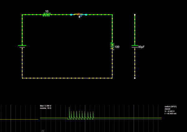
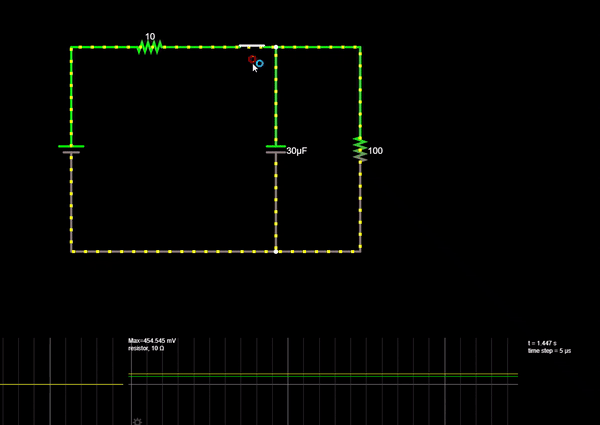
아무값을 넣어서 decap을 시뮬레이션 해보았다.
그리고 transient를 흉내내기 위해 인위적인 스위치를 계속 열고 닫아 전자의 흐름을 시뮬레이션 해보았다.
출처: https://electronics.stackexchange.com/questions/370320/how-to-place-decoupling-capacitors-on-a-four-layer-board-for-through-hole-componTransient가 되면 순간적으로 전류공급이 중단된다. (cap없을 때)Transient상태에도 전류 공급이 중단되지 않고 임시적으로 흐르게 된다. (cap이 병렬로 있을 때)
전선 간 인가하는 전압이 상승하다 전선 표면의 전위경도(Potential Gredient)가 위에 나온 공기의 절연내력(Dielectric Strength)을 넘어서는 순간, 전선 표면에 낮은 소리와 옅은 빛을 수반한 방전이 일어남.
- 코로나 방전으로 인한 문제 -
"코로나 손실"
코로나 방전으로 인해 발생하는 전력 손실로 전체적인 발전소 및 변전소의 효율을 감소 "코로나 잡음"
과도적(Transient)으로 발생하는 코로나 펄스(pulse)는 송전선로 근방에 있는 라디오/TV의 수신,반송 계전기,반송 통신 설비에 잡음을 유발
"코로나 장해"
코로나에 의한 고조파(Harmonic wave) 전류 중 제3고조파 성분은 중성점(Neutral Point) 전류로서 중성점 직접 접지 방식이 대부분인 우리나라 송전 선로 부근 통신선에 유도 장해(obstacle)를 일으킴
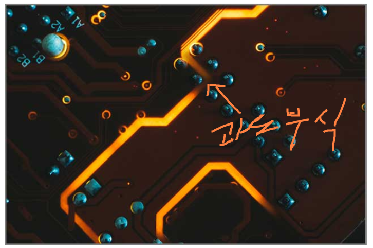
"전선의 부식 촉진"
코로나 방전이 화학작용이기 때문에 전선 지지점 등에서 전선의 부식을 발생
코로나 방전의 개념을 이해하려면 공기의 '절연내력'(air dielectric strength)도 알아야 합니다.절연내력이란 절연체에 어느 정도의 전압이 가해질 때 절연이 파괴되는지를 구한 한계값을 말합니다. 이 공식에 따라 공기의 절연내력을 계산해 보면 직류 전압이 인가될 땐 약30[kV/cm], 교류전압이 인가될 땐 약21[kV/cm]로 나타나는데요. 전선 간 인가하는 전압이 상승하다 전선 표면의 전위경도(Potential Gredient)가 위에 나온 공기의 절연내력(Dielectric Strength)을 넘어서는 순간,전선 표면에 낮은 소리와 옅은 빛을 수반한 방전이 일어나는 게 코로나 방전입니다.즉, 국부적으로 공기의 절연이 파괴되며 나타나는 방전현상이라 할 수 있습니다.
The purpose of the DRC is to cross check thePCB layoutdesign against the capabilities/constraints ofPCB fabricationshop. These constraints are communicated in terms of maximum tolerances to the PCB layout design engineer and the design engineer simply input these values to the DRC checker and Run DRC. As a result, any discrepancy is identified and rectified. The common constraints that DRC run can check are trace width, hole to trace clearance, overlaps, drill size, keep out, angle, blind via ratio and many others.
PCB제조업체의 허용치(제작 가능한가?)에 대한 Rule. 제조업체는 설계자에게 Rule을 전달하고, 설계자는 해당 Rule에 맞춰 설계를 진행해야 함. 모든 DRC조건이 만족할 때 비로소 설계데이터가 제조 가능. 일반적인 DRC 검사는 Trace 폭, 간격, 겹침, 드릴홀 크기, Keep out(이격거리), 각도, blind via 비율 등
Design For Manufacturing (DFM):
On the other hand, Design for Manufacturing (DFM) is a tool that can cover the grey areas that are left (remain unidentified) by DRC. This DFM (unlike DRC which is not an Ad-on but an integrated tool of CAD software) is an Ad-on provided for additional cost as an extra service by PCB fabricators to the customer. This can ultimately raise thecost of PCBbecause of DFM dedicated software is expensive and require manpower training. The DFM check will result in more qualified, reliable and high yield end product PCB.
DFM은 제조적인 관점에서 DRC체크로도 식별할 수 없는 영역을 탐지. 보통 add-on 툴로써 설계툴의 옵션으로 붙음.
일반적인 PCB설계보다 더 복잡한 정밀한 PCB설계를 위해 PCB제조업체가 추가적으로주는 디테일한 Rule.
1. Starved thermal pads
It is commonly observed that when reworking on a PCB during de-soldering the component from PCB, it takes lot of time, heat and effort. This is because the copper is a good conductor of heat. So when applying heat from soldering iron, the heat is wasted through the copper pour into the copper plane because the pad is completely surrounded by copper. So the component pad does not get enough heat to melt the solder and remove theelectronic component.
This issue is resolved by soldering the component on thermal pad. Thermal pad can have 2 or 4 thermal relief traces that connect the pad to the copper pour to copper plane. The air gap reduces the contact area so heat is not dissipated/wasted.
Now the design issue occurs when the thermal relief traces is not properly connected to copper pour or plane. The reason is the close proximity of multiple vias / pads or small spacing in between vias / pads. These small space may be cleared by DRC checker, but in actual the thermal relief traces will disturb the effected via and can displace vias from its copper pour.
납땜할 때 납의 녹는점을 유지하기 위한 온도가 중요, thermal relief 를 통해 열이 방출되는 시간을 조절할 수 있다. thermal relief trace가 얇으면 높은 온도가 오래 유지될 수 있고, 두껍다면 금방 열이 plane으로 방출되어 녹는점의 온도를 오래 유지하기 힘들다. 따라서 납땜이 잘되기 위한 적당한 두께를 지니도록 한다.
보통의 thermal pad는 airgap(흰색)을 두고 해당 pad와 copper plane간의 이격거리를 두어 급격한 열의 발산이 일어나지 않도록 도와준다.
2. Acid Traps Acute Angle
During the PCB design process, the design engineer can unknowingly makes a mistake. This mistake is that the two traces meet/cross each other at “acute angles” i.e less than 90 . As a result, the corners are made in the trace crossing point that can “trap” acid inside it. The acid referred here is the PCB etching solution used to etch away unwanted/excess copper from the PCB and only useful copper is left for making tracks/traces. This acid / etching solution is commonly available Ferric Chloride or Hydrochloric Acid.
The “acid trap hole” is another similar thing that arises due to very less gap between the trace and via. This will cause the space or pockets to form and retain the acid inside.
These acid if trapped for long time, can eat away copper trace and hence creates open circuit that can render the PCB board defective. The possibility of acid traps inmultilayer PCBis very high. Recent advancement in etching method (photo activated etching solution) of PCB has made this issue trivial but still best practice must be ensure to avoid acute angle traces.
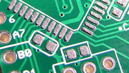
In some cases, like SOIC-08 IC package, the pad pitch is 5 mil and let’s suppose the fabrication min spec is 10mil so it can short copper pour and pad as shown in the figure. In this figure the upper pour diagram shows the copper pour has width 0.005 inch while lower pour is 0.016 inch. And you can see that the lower pour is not present between the pads of SOIC. In Eagle Software this can be done by changing the copper pour width. This is the good practice as shown in lower pour and upper pour shown is a mistake that a PCB designer can make
If this mistake is made, this can result in breakage of this very thin 5 mil trace in little pieces which can float in other components of PCB to create short circuit.
Pad의 Pitch(pad간 중심거리)가 5mil이고 제조업체의 사양이 10mil일 때, 위 그림의 윗부분의 pad사이에 있는 Copper pour에는 단락이 일어날 것이다. 이러한 실수가 발생하면 얇은 5mil 파편이 돌아다니면서 문제를 일으킬 수 있다.
즉, 제조업체의 최소 제작 사양을 확인하고 제작
4. Inadequate annular ring size
Thelayers of PCBare interconnected by means of vias. The vias are made by drilling the holes on both sides and then plating the walls of holes thus interconnecting the inner layers and two external layers (sides) of PCB.
Now if the pad size is very small then the holes bored will take the large space on pad leaving very narrow or inadequate ring size. This is called annular ring. This insufficient annular ring is caused by inaccuracy in drill bit position and inaccuracy in hitting the target to drill holes .
Pad의 크기가 매우작은 경우 drill hole이 차지하는 사이즈가 크게될 것인데, 이는 pad의 두께가 얇게 되어 올바른 Land Ring을 형성하기 힘듦. 그렇게 되면 Drill bit가 Hole을 뚦을때 살짝만 어긋나도 위와 같이 치우처진 via가 생성될 수 있음 (부적합한 갈고리 모양 via = annular ring)
적절한 Pad크기와 Hole의 크기를 지정해야 함)
5. Via in Pads
Sometimes it is important for PCB designer to place a via in Pad of a component. This is done for sake of compact PCB routing. In traditional routing, DRC error can raise due to drill size and trace width etc. So for small pitch components like sub 0.5mm it is inevitable to use a via in Pad as shown in figure.
However the drawback of this is that this via will work as a straw that will suck the solder away from the pad and will cause the inadequate soldering of component upon the pad. The solution to this problem is to use “Capped Via” as shown in this figure. Filling the conductive epoxy is also good.
전통적인 via생성 방식은 pad로 부터 튀어나와 via를 만들지만, 요즘처럼 부품의 크기가 작아져 pitch가 작아지는 경우에는 via를 pad위에 뚫는게 필수가 되고 있다. (위 그림처럼 "via in pad")
그러나 저런 경우 부품 납땜시 via hole을 통해 납을 흡수해버려 납땜이 잘 안된다. 그래서 저런 부분에는 Conductive epoxy소재로 가득채워 "Capped and Plated Via"를 만들어 사용한다.
6. Copper Layer near the board edge
The copper can be brought just close to the edge of PCB board because the design engineer does not include the “keep out layer” or “outline layer” in theGerber Files. This keep out layer is very important because if it is not included then the copper can be exposed to air and can cause trouble when boards are panelized resulting in short circuiting the copper layers. This feature can be easily caught in both DRC and DFM.
설계 엔지니어가 설계시 Board에 끝부분(outline)으로부터 이격거리(Keep out layer)를 설정하지 않는다면 Copper plane은 보드의 맨 끝부분(edge)까지 채워져 있을 것이다. 그런데 나중에 Panlize(여러 PCB보드를 자르는 것)을 하게되면 해당 Copper plane이 공기에 노출되는 문제가 있고, 또 Panlizing 과정중에 Short가 발생할 수도 있다.
따라서 설계시 Keep out layer 를 잘 지정하자 (DRC나 DFM 기능을 적절히 활용)
7. Missing solder mask between pads
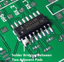
Solder mask is also called solder resist. It is used to protect the solder away from the copper track that you do not want to solder. For example in very small pitch components likeQFN package0.4mm pitch it is nearly impossible to apply solder mask in this tight space so it is common that you will not find solder mask because of standard DRC rules. This will result in a problem ofsolder bridgeas shown in figure.
납의 흐름을 방지시켜주는 soldermask(=solder resist)를 잘 적용해야 한다. QFN 패키지 같은 매우적은 pin간의 pitch(0.4mm)지닌 pad사이에서 솔더마스크가 없다면 Solder-Bridge(위 사진처럼 납땜하다 서로 연결되는)가 발생할 수 있다. 이점을 주의 한다.
8. Tombstoning
During the PCB assembly, when the small SMT passive components being soldered, the Tombstoning is caused by the improper wetting. When the solder paste starts to melt, an imbalanced torque at the ends of the component terminals causes the component to lift from one end. The component will be lifted from the end where the paste is wet. This Tombstoning can damage the PCB yields and raise cost of production. Other factors that cause Tombstoning are
An acid trap is simply any sharp corner in your trace pattern that could trap the harsh chemical etchants used to strip excess copper from a board during manufacture. When etching solution pools in a corner, there’s a risk of it tunneling through the etchant resist and corroding your traces and creating a faulty connection or open circuit.
acid trap을 요약하면 아래와 같이 분기하는 부분에 날카롭게 파인 코너 부에 etching(에칭) 가공시, 의도하지 않게 설계와 다르게 가공될 수 있다. (과도하게 Trace가 산화 되는 문제 등) 이러한 문제는 회로를 Open(단선) 또는 Short(단락, 합선)을 일으킬 수 있음.
즉 이 문제를 줄이기 위해서는 부드럽게 연결되지 않은 홈 부분의 이음세를 부드럽게 해주어야 한다.
During the PCB design process, the design engineer can unknowingly makes a mistake. This mistake is that the two traces meet/cross each other at “acute angles” i.e less than 90º . As a result, the corners are made in the trace crossing point that can “trap” acid inside it. The acid referred here is the PCB etching solution used to etch away unwanted/excess copper from the PCB and only useful copper is left for making tracks/traces. This acid / etching solution is commonly available Ferric Chloride or Hydrochloric Acid.
The “acid trap hole” is another similar thing that arises due to very less gap between the trace and via. This will cause the space or pockets to form and retain the acid inside.
These acid if trapped for long time, can eat away copper trace and hence creates open circuit that can render the PCB board defective. The possibility of acid traps inmultilayer PCBis very high. Recent advancement in etching method (photo activated etching solution) of PCB has made this issue trivial but still best practice must be ensure to avoid acute angle traces.
(간단 요약)
두 Trace가 "acute angle", 즉 90º 미만에서 서로 만나거나 교차할 때, Etching 작업 시, 모서리 사이에 좀 과한 산 용액이 남게 되어 과하게 부식이 될 수 있다. (주로 사용되는 etching 성분은 염화철 또는 염산)
"Acid trap hole"은 trace와 via 사이의 간격이 매우 적을때 발생. 이 hole로 인해 산 용액이 해당 자리에 머물며 부식 시킴. 이는 Trace를 부식시켜 Open(단선) 시킬 수 있음