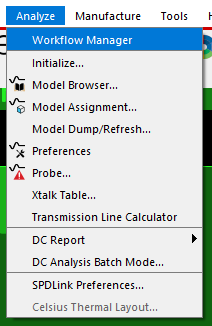
Printed Circuit Boards (PCBs) have been the focus of scientist and engineers to bring novel ideas on how to improve the quality of end electronic product. As PCBs play the key role in functionality and performance of any electronic product or device so the perfectly designed PCB layout is highly important. There are many factors that a design engineer must consider while designing a PCB layout and these factors are driven by the requirements of end product.
Like number of layers PCB, size and dimensions of PCB, number of electronic components to be soldered upon PCB, types of components, routing techniques and many other PCB design factors. Among them one of the most important aspect is the “Impedance Matching”. The PCB that is dedicated for the electronic product that is to be used for High frequency application like RF or microwave electronics, then the most critical part of the PCB layout design is to control the impedance of the circuit.
인쇄 회로 기판(PCB)의 주 초점은 최종 전자제품의 품질을 개선하는 방법에 대한 아이디어를 과학자와 엔지니어가 함께 고안하는 것이 주요 관점이었다. PCB는 모든 전자 제품의 기능 및 성능에서 핵심적인 역할을 하므로 완벽하게 설계된 PCB 레이아웃이 중요하다. 설계 엔지니어가 PCB 레이아웃을 설계할 때 고려해야 하는 많은 요소가 있으며 이러한 요소는 최종 제품의 요구 사항에 따라 결정된다.
PCB 레이어 수, PCB 크기 및 치수, PCB에 납땜할 부품 수, 부품의 유형, 배선 기술 및 기타 여러 요소 등, 그 중 가장 중요한 요소 중 하나는 "임피던스 매칭" 이다. RF나 microwave와 같은 고주파를 응용 분야에 사용되는 전용 PCB에서 가장 중요한 부분은 회로의 임피던스를 제어하는 것이다.
What is Signal Reflection.?
As we are familiar with the phenomena of reflection that when a light ray is incident on the mirror then the light is reflected from mirror’s surface. Another example is water, when light enters the water some of the light is refracted while some is reflected. The same phenomena is with electrical signal.
The signal reflection is the phenomena where the source transmits the electrical signal in the signal trace to the receiver/sink and some part of the signal is reflected back from receiver/sink back to the source. This reflected signal can cause signal distortion and oscillation in the circuit.
신호반사란?
우리는 보통 반사 현상에 익숙한데, 광선(빛)이 거울에 입사하면 빛이 거울 표면에서 반사가 일어난다. 또 다른 예로는 물이다. 빛이 물에 들어갈 때 빛의 일부는 굴절되고 일부는 반사된다. 이와 동일한 현상이 전기 신호에서도 발생한다.
신호 반사는 신호원(Source)가 신호 선로(Trace)상의 전기 신호를 수신기(Receiver 또는 Sink)에 전송하고, 신호의 일부가 다시 신호원(Source)로 반사되는 현상이다. 이 반사된 신호는 회로상의 신호 왜곡(Signal distortion) 또는 발진(oscillation)을 일으킬 수 있다.
Why the Signal is reflected..?
The reason for the signal reflection from receiver to the transmitter is the transient impedance caused by the discontinuity in characteristic impedance of signal trace. If the characteristic impedance is uniform through starting from source or transmitter to sink or receiver then there will be no signal reflection.
The discontinuity in characteristic impedance of signal trace can be caused by variation in signal trace width, thickness, distance between the trace and the corresponding reference plane and dielectric constant of the substrate material of PCB.
왜 신호반사가 일어나는 걸까?
수신기(reciever)에서 송신기(transmitter)로 신호가 반사되는 이유는 신호 트레이스의 특성임피던스(characteristic impedance)의 불연속성으로 인해 발생하는 과도임피던스(transient impedance)이다. 특성 임피던스가 신호원(Source / transmitter)에서 수신기(Receiver 또는 Sink)로 균일한 임피던스일 경우 신호 반사가 없다.
반면에 트레이스(trace)의 특성 임피던스의 불연속성은 신호 트레이스 폭, 두께, 트레이스와 해당 기준 평면 사이의 거리 및 PCB 기판 재료의 유전 상수의 변화로 인해 발생할 수 있다 .
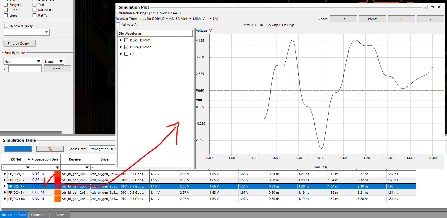
Fortunately, the signal reflected from receiver is always less in strength then the main signal, hence the reflected signal is again transmitted and then again reflected with lesser strength, and hence in this way the signal is diminished slowly but will cause a temporary oscillation.
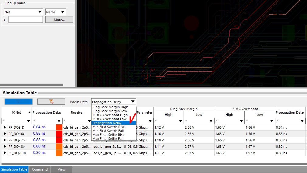
Overshooting and Undershooting:
If the delay time between the signal transmission and reception is short and the signal transmission is faster and if the previous reflected signal was not given time/delay to diminish and next signal is transmitted then this will cause the signal “peaks” to accumulate and will cause reflected signal overshooting thus complete failure of the circuit will happen. Similarly if the signal “valley” are accumulated this will cause reflected signal undershooting thus weakening the main signal to cause false clocking or misinterpretation of digital data lines like SDI, SDO, SCLK etc. This overshooting or undershooting can completely destroy the protective diodes at the signal ends.
Signal Distortion:
The reflected signals from receiver end if are strong enough then they can possibly change the logic state of digital circuitry hence the circuit will behave in unanticipated manner. Distorted signal are sensitive towards noise.
신호 반사의 효과:
발진(Oscillation):
다행이도 수신기로부터 반사된 신호(reflected signal)는 항상 주신호(main signal)보다 강도가 낮기 때문에, 반사된 신호는 왔다 갔다 점점 약한 강도가 되어 점점 감소하지만, 이는 일시적인 진동을 일으킨다.
오버슈팅, 언더슈팅 (Overshooting and Undershooting:):
신호의 전송과 수신 사이의 지연 시간이 짧고, 신호가 빨라서 반사된 신호가 감쇄를 일으킬 시간을 충분히 주지 않는 상태에서 다음 신호가 전송되면, 신호 "피크(peak)"가 누적되어 결국 반사 신호 오버슈팅을 유발하여 회로의 완전한 고장이 발생한다.
비슷하게 "밸리(valley)" 신호가 누적되면 반사 신호 언더슈팅이 발생하여 주 신호(main signal)를 약화시켜 SDI, SDO, SCLK 등과 같은 디지털 데이터 라인의 잘못된 클럭(clock) 또는 신호의 잘못된 해석(misinterpretation)을 유발한다. 이러한 오버슈팅 또는 언더슈팅은 보호 다이오드에서 보호 다이오드를 완전히 파괴되어 신호가 종료될 수 있다.